1. Crystal Structure and Split Anisotropy
1.1 The 2H and 1T Polymorphs: Architectural and Digital Duality
(Molybdenum Disulfide)
Molybdenum disulfide (MoS ₂) is a layered shift metal dichalcogenide (TMD) with a chemical formula including one molybdenum atom sandwiched between 2 sulfur atoms in a trigonal prismatic control, creating covalently adhered S– Mo– S sheets.
These specific monolayers are piled up and down and held together by weak van der Waals pressures, making it possible for very easy interlayer shear and peeling down to atomically slim two-dimensional (2D) crystals– an architectural function central to its diverse practical roles.
MoS two exists in multiple polymorphic forms, one of the most thermodynamically steady being the semiconducting 2H phase (hexagonal symmetry), where each layer shows a straight bandgap of ~ 1.8 eV in monolayer type that transitions to an indirect bandgap (~ 1.3 eV) in bulk, a phenomenon crucial for optoelectronic applications.
On the other hand, the metastable 1T stage (tetragonal balance) takes on an octahedral sychronisation and behaves as a metallic conductor as a result of electron contribution from the sulfur atoms, allowing applications in electrocatalysis and conductive compounds.
Phase changes in between 2H and 1T can be generated chemically, electrochemically, or via stress design, supplying a tunable platform for making multifunctional devices.
The ability to stabilize and pattern these stages spatially within a solitary flake opens up paths for in-plane heterostructures with distinctive digital domain names.
1.2 Issues, Doping, and Edge States
The performance of MoS ₂ in catalytic and electronic applications is extremely sensitive to atomic-scale defects and dopants.
Innate point flaws such as sulfur vacancies function as electron benefactors, boosting n-type conductivity and functioning as active sites for hydrogen evolution reactions (HER) in water splitting.
Grain borders and line defects can either restrain cost transport or produce local conductive paths, depending on their atomic configuration.
Managed doping with change steels (e.g., Re, Nb) or chalcogens (e.g., Se) allows fine-tuning of the band framework, service provider focus, and spin-orbit combining impacts.
Significantly, the edges of MoS ₂ nanosheets, especially the metal Mo-terminated (10– 10) sides, show substantially higher catalytic task than the inert basal airplane, inspiring the layout of nanostructured drivers with made best use of side exposure.
( Molybdenum Disulfide)
These defect-engineered systems exemplify exactly how atomic-level control can change a normally taking place mineral into a high-performance practical product.
2. Synthesis and Nanofabrication Strategies
2.1 Bulk and Thin-Film Production Techniques
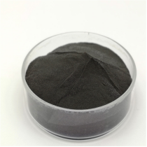
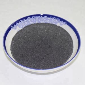
Natural molybdenite, the mineral kind of MoS TWO, has been used for decades as a solid lubricating substance, yet contemporary applications require high-purity, structurally regulated artificial types.
Chemical vapor deposition (CVD) is the dominant approach for generating large-area, high-crystallinity monolayer and few-layer MoS ₂ films on substrates such as SiO TWO/ Si, sapphire, or versatile polymers.
In CVD, molybdenum and sulfur precursors (e.g., MoO ₃ and S powder) are vaporized at heats (700– 1000 ° C )in control environments, allowing layer-by-layer growth with tunable domain name dimension and orientation.
Mechanical peeling (“scotch tape technique”) remains a criteria for research-grade samples, producing ultra-clean monolayers with very little problems, though it lacks scalability.
Liquid-phase exfoliation, including sonication or shear blending of mass crystals in solvents or surfactant options, creates colloidal dispersions of few-layer nanosheets appropriate for finishings, composites, and ink formulations.
2.2 Heterostructure Integration and Device Patterning
Real capacity of MoS ₂ arises when integrated right into vertical or side heterostructures with other 2D products such as graphene, hexagonal boron nitride (h-BN), or WSe two.
These van der Waals heterostructures make it possible for the style of atomically precise devices, consisting of tunneling transistors, photodetectors, and light-emitting diodes (LEDs), where interlayer fee and energy transfer can be crafted.
Lithographic patterning and etching strategies enable the fabrication of nanoribbons, quantum dots, and field-effect transistors (FETs) with network sizes to 10s of nanometers.
Dielectric encapsulation with h-BN secures MoS two from ecological deterioration and minimizes fee scattering, considerably improving provider mobility and gadget security.
These manufacture breakthroughs are essential for transitioning MoS ₂ from lab inquisitiveness to practical part in next-generation nanoelectronics.
3. Practical Features and Physical Mechanisms
3.1 Tribological Habits and Solid Lubrication
One of the oldest and most enduring applications of MoS two is as a completely dry solid lube in extreme environments where fluid oils stop working– such as vacuum cleaner, heats, or cryogenic conditions.
The low interlayer shear stamina of the van der Waals space enables easy sliding between S– Mo– S layers, resulting in a coefficient of friction as reduced as 0.03– 0.06 under optimum conditions.
Its efficiency is additionally improved by strong adhesion to metal surfaces and resistance to oxidation as much as ~ 350 ° C in air, past which MoO ₃ formation raises wear.
MoS two is commonly utilized in aerospace mechanisms, air pump, and gun components, usually applied as a layer via burnishing, sputtering, or composite unification into polymer matrices.
Recent research studies reveal that humidity can break down lubricity by boosting interlayer adhesion, prompting study into hydrophobic coatings or hybrid lubricating substances for enhanced ecological security.
3.2 Electronic and Optoelectronic Feedback
As a direct-gap semiconductor in monolayer form, MoS two displays solid light-matter communication, with absorption coefficients going beyond 10 ⁵ cm ⁻¹ and high quantum return in photoluminescence.
This makes it ideal for ultrathin photodetectors with quick feedback times and broadband level of sensitivity, from noticeable to near-infrared wavelengths.
Field-effect transistors based upon monolayer MoS ₂ demonstrate on/off proportions > 10 ⁸ and service provider flexibilities as much as 500 cm ²/ V · s in put on hold samples, though substrate interactions commonly restrict sensible worths to 1– 20 centimeters ²/ V · s.
Spin-valley combining, a consequence of strong spin-orbit interaction and broken inversion proportion, enables valleytronics– a novel paradigm for information inscribing utilizing the valley level of liberty in energy space.
These quantum sensations setting MoS two as a prospect for low-power reasoning, memory, and quantum computing elements.
4. Applications in Power, Catalysis, and Emerging Technologies
4.1 Electrocatalysis for Hydrogen Evolution Reaction (HER)
MoS ₂ has become a promising non-precious choice to platinum in the hydrogen development reaction (HER), an essential process in water electrolysis for eco-friendly hydrogen manufacturing.
While the basic airplane is catalytically inert, edge websites and sulfur openings exhibit near-optimal hydrogen adsorption totally free energy (ΔG_H * ≈ 0), comparable to Pt.
Nanostructuring techniques– such as producing vertically aligned nanosheets, defect-rich movies, or doped hybrids with Ni or Co– make the most of energetic website density and electrical conductivity.
When incorporated right into electrodes with conductive supports like carbon nanotubes or graphene, MoS two attains high existing thickness and long-term stability under acidic or neutral conditions.
Further improvement is achieved by maintaining the metal 1T phase, which improves intrinsic conductivity and subjects added energetic sites.
4.2 Adaptable Electronic Devices, Sensors, and Quantum Instruments
The mechanical adaptability, openness, and high surface-to-volume ratio of MoS ₂ make it suitable for adaptable and wearable electronic devices.
Transistors, reasoning circuits, and memory tools have actually been shown on plastic substratums, enabling bendable displays, health and wellness displays, and IoT sensors.
MoS ₂-based gas sensing units show high level of sensitivity to NO TWO, NH FOUR, and H TWO O due to charge transfer upon molecular adsorption, with reaction times in the sub-second array.
In quantum modern technologies, MoS two hosts localized excitons and trions at cryogenic temperature levels, and strain-induced pseudomagnetic areas can catch providers, allowing single-photon emitters and quantum dots.
These developments highlight MoS ₂ not just as a useful product yet as a platform for exploring fundamental physics in decreased dimensions.
In summary, molybdenum disulfide exemplifies the convergence of timeless materials science and quantum design.
From its old function as a lubricating substance to its modern release in atomically thin electronic devices and power systems, MoS ₂ remains to redefine the limits of what is feasible in nanoscale materials design.
As synthesis, characterization, and assimilation methods advancement, its impact across science and innovation is poised to expand even further.
5. Supplier
TRUNNANO is a globally recognized Molybdenum Disulfide manufacturer and supplier of compounds with more than 12 years of expertise in the highest quality nanomaterials and other chemicals. The company develops a variety of powder materials and chemicals. Provide OEM service. If you need high quality Molybdenum Disulfide, please feel free to contact us. You can click on the product to contact us.
Tags: Molybdenum Disulfide, nano molybdenum disulfide, MoS2
All articles and pictures are from the Internet. If there are any copyright issues, please contact us in time to delete.
Inquiry us