1. Crystal Framework and Polytypism of Silicon Carbide
1.1 Cubic and Hexagonal Polytypes: From 3C to 6H and Beyond
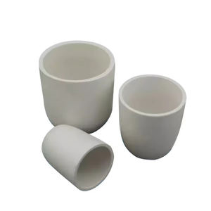
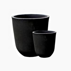
(Silicon Carbide Ceramics)
Silicon carbide (SiC) is a covalently bonded ceramic made up of silicon and carbon atoms arranged in a tetrahedral control, forming among one of the most intricate systems of polytypism in products scientific research.
Unlike a lot of ceramics with a single stable crystal framework, SiC exists in over 250 recognized polytypes– distinct piling sequences of close-packed Si-C bilayers along the c-axis– varying from cubic 3C-SiC (additionally called β-SiC) to hexagonal 6H-SiC and rhombohedral 15R-SiC.
One of the most typical polytypes used in engineering applications are 3C (cubic), 4H, and 6H (both hexagonal), each displaying slightly various digital band frameworks and thermal conductivities.
3C-SiC, with its zinc blende structure, has the narrowest bandgap (~ 2.3 eV) and is normally grown on silicon substrates for semiconductor tools, while 4H-SiC supplies premium electron flexibility and is preferred for high-power electronics.
The strong covalent bonding and directional nature of the Si– C bond give remarkable hardness, thermal stability, and resistance to slip and chemical assault, making SiC suitable for severe atmosphere applications.
1.2 Problems, Doping, and Electronic Feature
Despite its structural complexity, SiC can be doped to accomplish both n-type and p-type conductivity, enabling its usage in semiconductor gadgets.
Nitrogen and phosphorus work as benefactor pollutants, introducing electrons into the conduction band, while aluminum and boron work as acceptors, developing holes in the valence band.
Nonetheless, p-type doping performance is limited by high activation powers, especially in 4H-SiC, which presents challenges for bipolar device design.
Indigenous issues such as screw misplacements, micropipes, and piling mistakes can deteriorate device performance by functioning as recombination centers or leakage paths, necessitating top quality single-crystal development for digital applications.
The vast bandgap (2.3– 3.3 eV depending upon polytype), high breakdown electric area (~ 3 MV/cm), and outstanding thermal conductivity (~ 3– 4 W/m · K for 4H-SiC) make SiC much above silicon in high-temperature, high-voltage, and high-frequency power electronic devices.
2. Processing and Microstructural Engineering
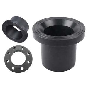
( Silicon Carbide Ceramics)
2.1 Sintering and Densification Methods
Silicon carbide is inherently hard to densify as a result of its solid covalent bonding and low self-diffusion coefficients, requiring innovative processing methods to achieve full density without additives or with marginal sintering aids.
Pressureless sintering of submicron SiC powders is feasible with the addition of boron and carbon, which promote densification by removing oxide layers and improving solid-state diffusion.
Hot pressing applies uniaxial pressure throughout heating, enabling full densification at reduced temperature levels (~ 1800– 2000 ° C )and producing fine-grained, high-strength components suitable for cutting devices and wear components.
For huge or complicated shapes, response bonding is used, where permeable carbon preforms are infiltrated with liquified silicon at ~ 1600 ° C, developing β-SiC sitting with marginal shrinking.
However, recurring complimentary silicon (~ 5– 10%) remains in the microstructure, restricting high-temperature efficiency and oxidation resistance above 1300 ° C.
2.2 Additive Production and Near-Net-Shape Fabrication
Recent developments in additive manufacturing (AM), particularly binder jetting and stereolithography making use of SiC powders or preceramic polymers, allow the fabrication of complicated geometries previously unattainable with traditional methods.
In polymer-derived ceramic (PDC) routes, liquid SiC precursors are formed via 3D printing and afterwards pyrolyzed at high temperatures to produce amorphous or nanocrystalline SiC, frequently calling for additional densification.
These techniques reduce machining costs and material waste, making SiC a lot more obtainable for aerospace, nuclear, and warmth exchanger applications where intricate layouts enhance efficiency.
Post-processing steps such as chemical vapor infiltration (CVI) or fluid silicon infiltration (LSI) are in some cases utilized to boost density and mechanical integrity.
3. Mechanical, Thermal, and Environmental Performance
3.1 Toughness, Hardness, and Use Resistance
Silicon carbide rates amongst the hardest well-known materials, with a Mohs firmness of ~ 9.5 and Vickers firmness surpassing 25 GPa, making it extremely resistant to abrasion, disintegration, and scratching.
Its flexural toughness commonly varies from 300 to 600 MPa, depending on handling approach and grain dimension, and it keeps stamina at temperatures approximately 1400 ° C in inert atmospheres.
Fracture durability, while modest (~ 3– 4 MPa · m ONE/ TWO), suffices for many architectural applications, particularly when integrated with fiber reinforcement in ceramic matrix composites (CMCs).
SiC-based CMCs are used in wind turbine blades, combustor liners, and brake systems, where they supply weight financial savings, fuel effectiveness, and extended life span over metal equivalents.
Its outstanding wear resistance makes SiC ideal for seals, bearings, pump parts, and ballistic shield, where longevity under extreme mechanical loading is essential.
3.2 Thermal Conductivity and Oxidation Stability
One of SiC’s most useful residential properties is its high thermal conductivity– as much as 490 W/m · K for single-crystal 4H-SiC and ~ 30– 120 W/m · K for polycrystalline types– surpassing that of many metals and enabling reliable warmth dissipation.
This residential property is crucial in power electronic devices, where SiC gadgets produce less waste warm and can operate at higher power thickness than silicon-based gadgets.
At raised temperature levels in oxidizing environments, SiC develops a protective silica (SiO TWO) layer that slows additional oxidation, providing great environmental durability up to ~ 1600 ° C.
Nonetheless, in water vapor-rich atmospheres, this layer can volatilize as Si(OH)FOUR, resulting in accelerated degradation– a vital difficulty in gas wind turbine applications.
4. Advanced Applications in Power, Electronic Devices, and Aerospace
4.1 Power Electronics and Semiconductor Tools
Silicon carbide has reinvented power electronics by making it possible for gadgets such as Schottky diodes, MOSFETs, and JFETs that run at higher voltages, frequencies, and temperature levels than silicon matchings.
These gadgets lower power losses in electric vehicles, renewable energy inverters, and industrial motor drives, contributing to worldwide energy effectiveness renovations.
The capacity to run at junction temperature levels above 200 ° C permits streamlined cooling systems and raised system reliability.
Moreover, SiC wafers are used as substratums for gallium nitride (GaN) epitaxy in high-electron-mobility transistors (HEMTs), incorporating the advantages of both wide-bandgap semiconductors.
4.2 Nuclear, Aerospace, and Optical Equipments
In atomic power plants, SiC is a crucial component of accident-tolerant gas cladding, where its reduced neutron absorption cross-section, radiation resistance, and high-temperature toughness enhance security and efficiency.
In aerospace, SiC fiber-reinforced composites are utilized in jet engines and hypersonic vehicles for their lightweight and thermal stability.
In addition, ultra-smooth SiC mirrors are employed precede telescopes due to their high stiffness-to-density proportion, thermal stability, and polishability to sub-nanometer roughness.
In recap, silicon carbide ceramics stand for a foundation of contemporary innovative materials, incorporating remarkable mechanical, thermal, and digital properties.
With specific control of polytype, microstructure, and handling, SiC continues to allow technical advancements in energy, transport, and extreme setting design.
5. Provider
TRUNNANO is a supplier of Spherical Tungsten Powder with over 12 years of experience in nano-building energy conservation and nanotechnology development. It accepts payment via Credit Card, T/T, West Union and Paypal. Trunnano will ship the goods to customers overseas through FedEx, DHL, by air, or by sea. If you want to know more about Spherical Tungsten Powder, please feel free to contact us and send an inquiry(sales5@nanotrun.com).
Tags: silicon carbide ceramic,silicon carbide ceramic products, industry ceramic
All articles and pictures are from the Internet. If there are any copyright issues, please contact us in time to delete.
Inquiry us